
Ministry of Electronics & Information Technology
(MeitY)
Chips to Startup (C2S)

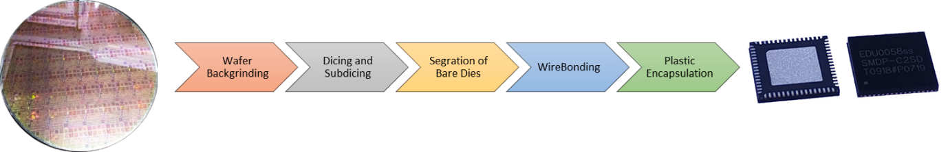
Chip Centre was established at C-DAC, Bangalore for undertaking Siliconization of ASICs/Integrated Circuits designed by Special Development Programme-Chips to System design (SMDP-C2SD) Institutions. Chip Centre was the nodal centre for integrating the designs received from institutions and sending them to Semi-Conductor Laboratory (SCL), Chandigarh for fabrication in MPW mode. Chip Centre also facilitated the Institutions in packaging of bare dies received from SCL.
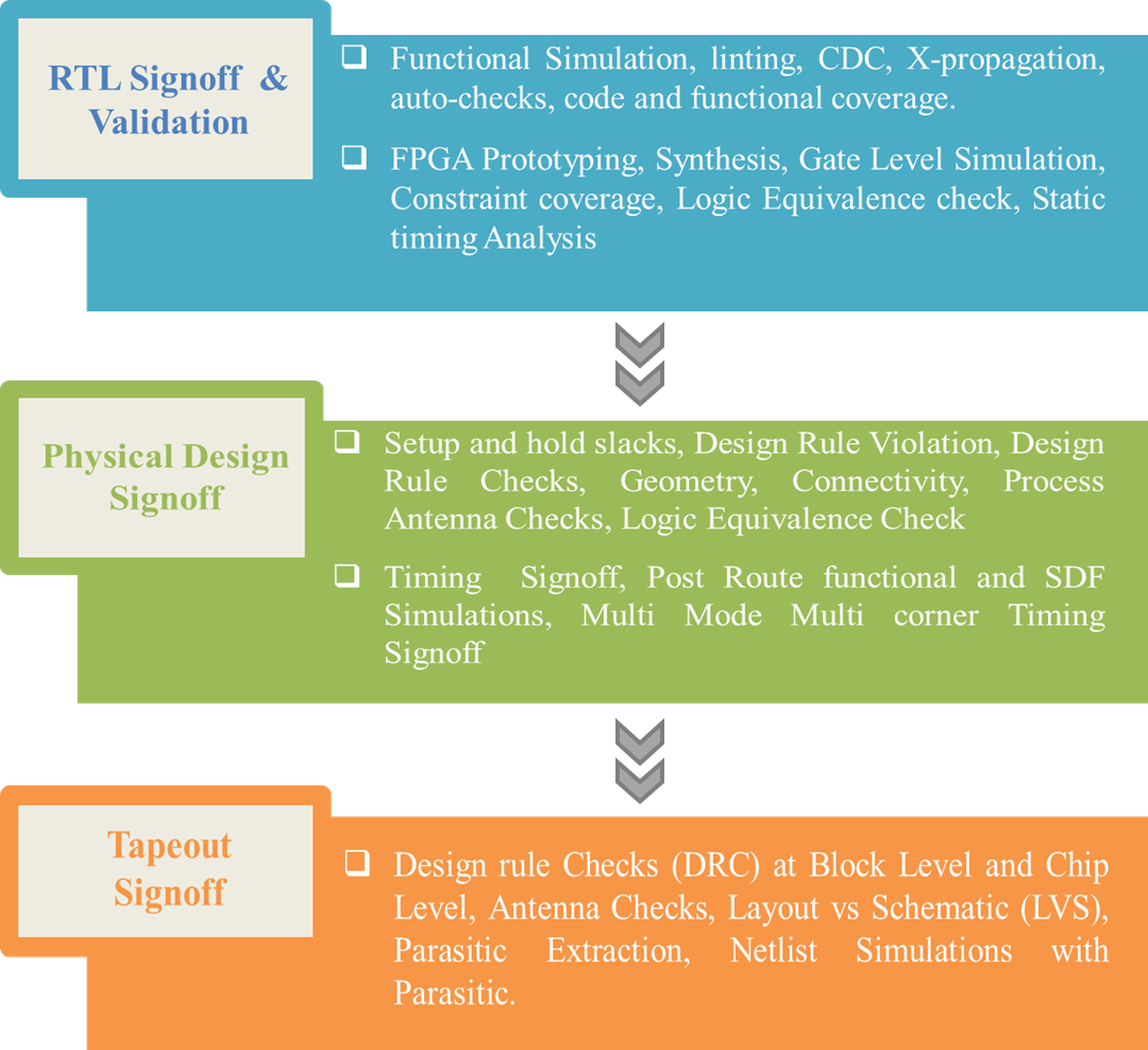
In order to provide exposure of complete VLSI design cycle to all Participating Institutions from specification to Fab tape out, it is upgraded to the capability and responsibility of existing Chip Centre and to establish a design Centre as part of Chip Centre for providing design support to the Institutions and Start-ups for development of ASIC and FPGA based designs.
Under current C2S programme, India Chip Centre will provide fabrication support at SCL and overseas foundries in MPW mode to Institutions/Start-ups/MSMEs. It also offer design services including maintaining IP Core Repository, Design flow establishment with a specific set of EDA tools and the Fab Process Design Kit (PDK) , Fab compliance validation of Designs, Packaging of Chips, Testing, Characterization in the Country in centralized manner.


Content owned & provided by Ministry of Electronics & Information Technology, Government of India
Website visitor count (since 17th Feb 2025): 1961486
